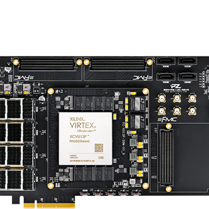
Interface Function Display
 Puzhi FPGA ZYNQ7000 ZYNQ7010 Development BoardPZ7010-KFB
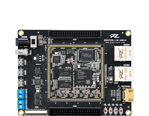 Puzhi FPGA ZYNQ7000 ZYNQ7020 Development BoardPZ7020-KFB
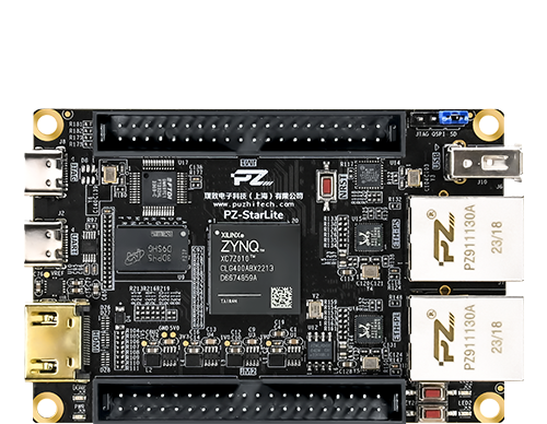 Puzhi FPGA ZYNQ7000 PZ7010-StarLite Development BoardPZ7010-StarLite
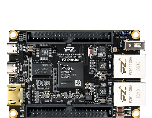 Puzhi FPGA ZYNQ7000 PZ7020-StarLite Development BoardPZ7020-StarLite
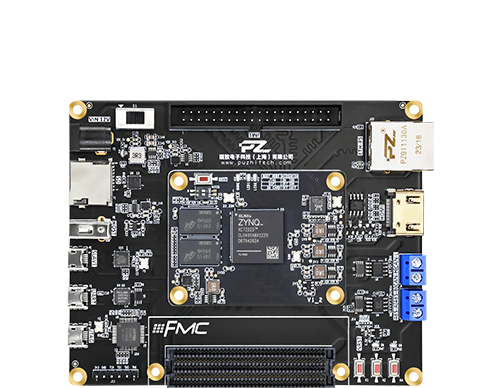 Puzhi FPGA ZYNQ7000 PZ7020S-FL Development BoardPZ7020S-FL-KFB
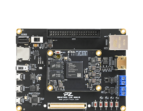 Puzhi FPGA ZYNQ7000 ZYNQ7010S Development BoardPZ7010S-KFB
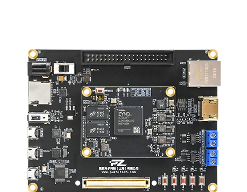 Puzhi FPGA ZYNQ7000 ZYNQ7020S Development BoardPZ7020S-KFB
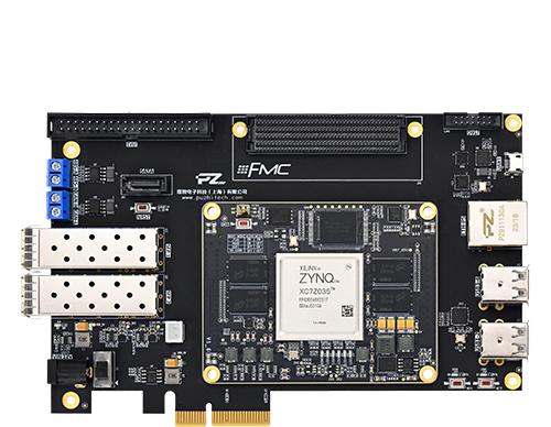 Puzhi FPGA ZYNQ7000 PZ7035-FH Development BoardPZ7035-FH-KFB
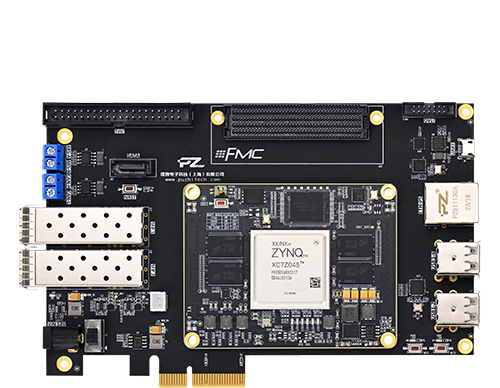 Puzhi FPGA ZYNQ7000 PZ7045-FH Development BoardPZ7045-FH-KFB
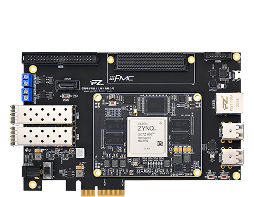 Puzhi FPGA ZYNQ7000 PZ7100-FH Development BoardPZ7100-FH-KFB
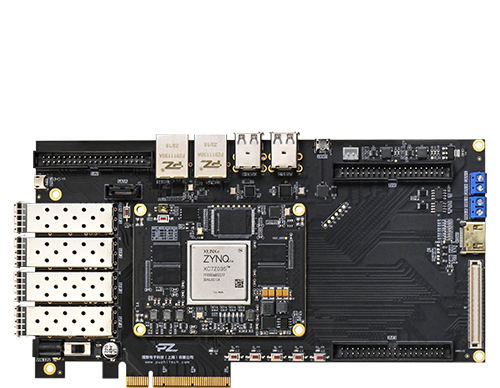 Puzhi FPGA ZYNQ7000 ZYNQ7035 Development BoardPZ7035-KFB-900
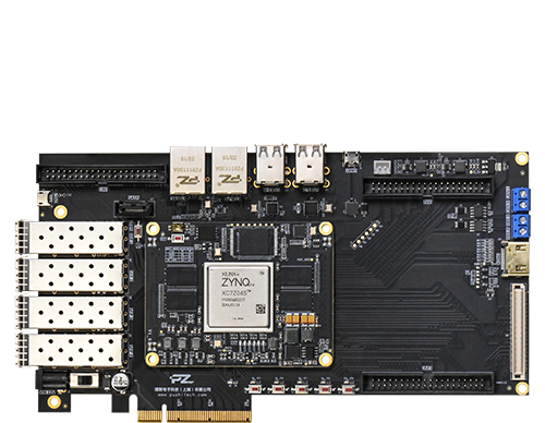 Puzhi FPGA ZYNQ7000 ZYNQ7045 Development BoardPZ7045-KFB-900
Product Parameters
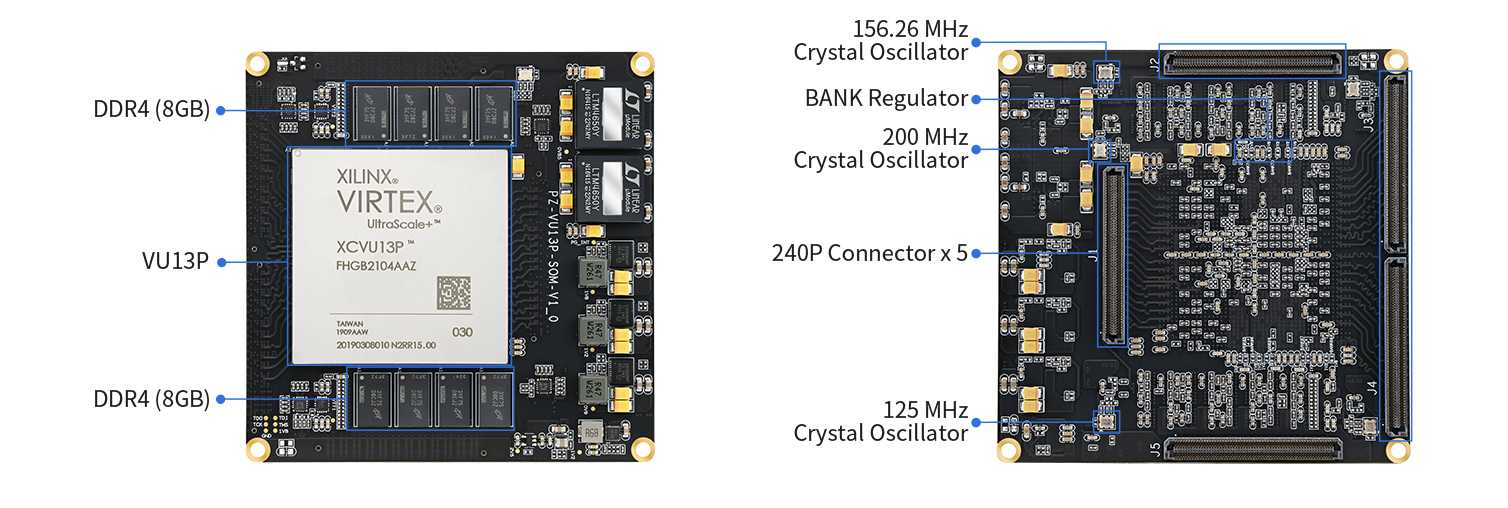
Core Board Main Parameters
FPGA Dev. Board | PZ-VU13P-KFB |
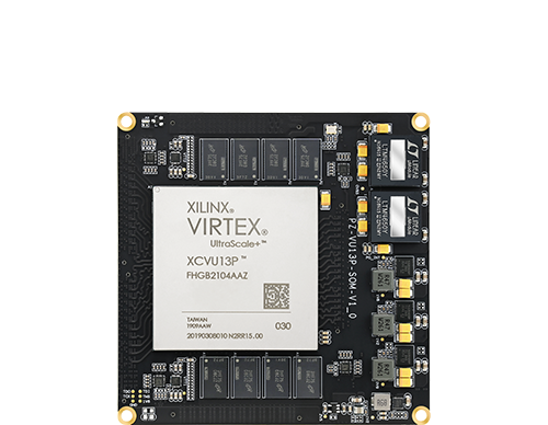
FPGA Chip | XCVU13P-2FLGB2104I |
Speed Grade | 2 |
Chip Level | Industrial Grade(-40°C~+85°C) |
Logic Cells | 3780k |
Lookup Tables | 1728k |
Flip-Flops | 3456k |
DSP Slices | 12288 |
BLOCK RAM | 94.5Mb |
DDR4 | Dual Group of DDR4 (8GB+8GB) |
Start-up Mode | JTAG/ BPI/ SPI, JTAG Startup by default |
Number of IO | 360 single-ended/180 differential pairs (1.2/1.8V adjustable, default 1.8V) |
Number of GTY | 76 Pairs of TX/RX |
Crystal Oscillator | 200MHz Differential Crystal for FPGA 125MHz and 156.25MHz Differential Crystal for the GT Transceiver Reference Clock |
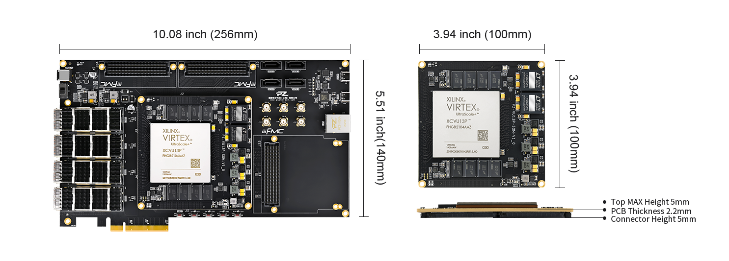
Core Board Form Factors | 3.94 inch x 3.94 inch (100mm x 100mm) |
Interfaces and Function
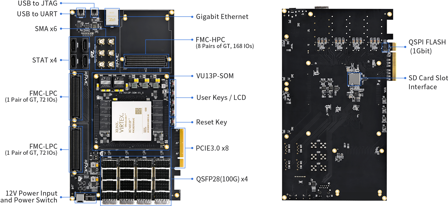
JTAG Downloader | 1 |
UART | 1 |
Gigabit Ethernet | 1 |
PICE3.0 | x8 |
QSFP28 | 4 x 100G |
FMC Interface | HPC (8 Pairs of GT, 168 IOs), 2 LPC (1Pair of GT, 72 IOs) |
Voltage / Current | 12V / 20A |
Board Form Factors | 10.08 inch x 5.51 inch (256mm x 140mm) |
Technology | Black Matte. Immersion Gold Process |
Product Dimensions
Product Packages
FMC Subcard Display
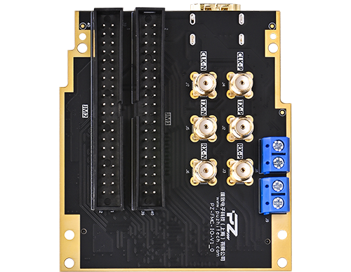
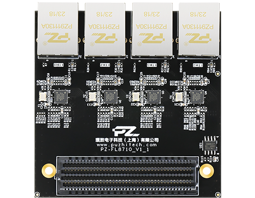
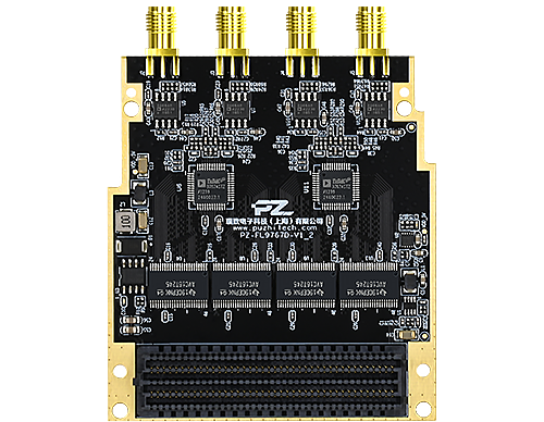
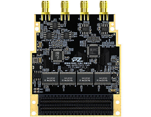
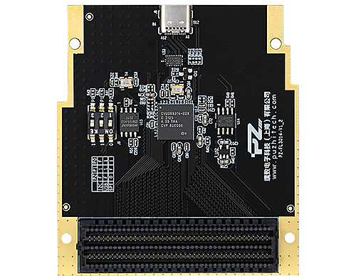
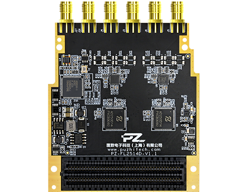
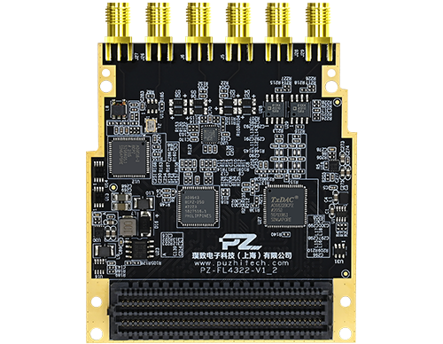
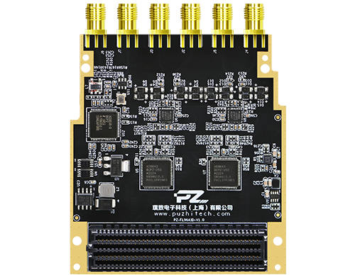
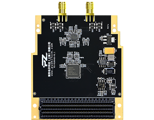
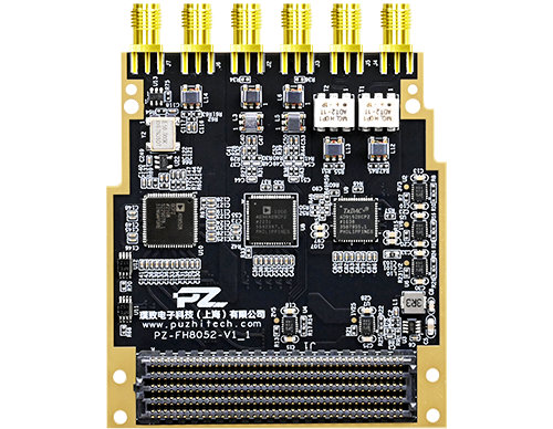
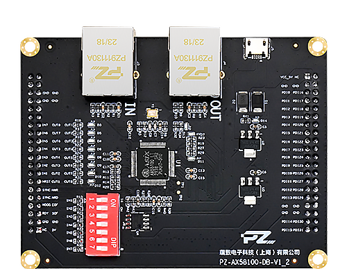
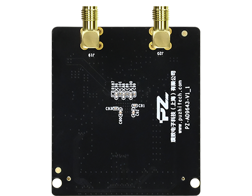
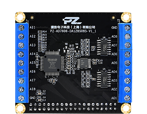
Other Subcard Display
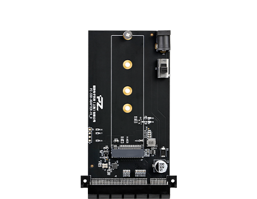
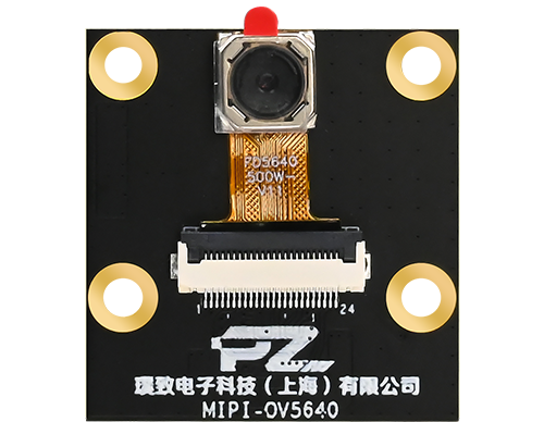
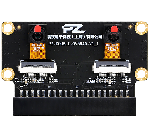
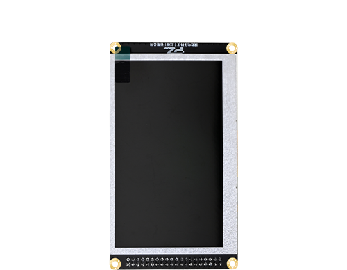
Demos Come with the Board
Contact Customer Service after Purchase Files Saved in Google Drive/ Yandex/ Dropbox
Demos Constantly Being Updated... ...
- 1
FPGA Logic Demos
- 01.
Vivado Installation
- 02.
FLASH Curing
- 03.
LED Flashing
- 04.
LED PWM Control
- 05.
Key Control LED
- 06.
FPGA on-chip RAM Read and Write
- 07.
FPGA on-chip ROM Read and Write
- 08.
FPGA on-chip PLL Configuration
- 09.
FPGA on-chip FIFO Read and Write
- 10.
FPGA side DDR4 Control Read and Write
- 11.
I2C Read and Write E2PROM
- 12.
Uart Transceiver
- 13.
SD Card Read and Write
- 14.
Gigabit UDP Based on RTL8211
- 15.
SFP Bit Error Rate
- 16.
PCIE Speed Test
- 17.
Aurora Communication
- 18.
High Speed ADC-AD9643 Acquisition (250MSPS)
- 19.
UDP Transmission of High-speed ADC Acquisition Data
- 01.
- 2
Microblaze Parts
- 01.
Microblaze LED
- 02.
Microblaze Uart
- 03.
Microblaze GPIO Interrupt
- 04.
Microblaze Timer Interrupt
- 05.
Microblaze DMA LOOP
- 06.
Microblaze XADC
- 07.
Microblaze Lwip TCP loop
- 01.
- 3
FMC Topics(FMC daughter board is required)
- 01.
USB3.0 (PZ-FL3014)
- 02.
High Speed ADC (PZ-FL9643S)
- 03.
High Speed ADC/DAC (PZ-FL4322)
- 04.
Multi-Channel High-Speed ADC (PZ-FL9643D)
- 05.
Multi-Channel Domestic High-Speed (PZ-FL2514D)
- 06.
Ultra High Speed ADC/DAC (PZ-FH8052)
- 07.
Medium-Speed ADC/DAC (PZ-FL3867)
- 08.
Multi-Channel Medium Speed DAC (PZ-FL9767D)
- 09.
Quad 100Gb Ethernet (PZ-FL8710F)
- 10.
Quad 1000Gb Ethernet (PZ-FL8211F)
- 11.
Software Defined Radio(PZ-FL9361/PZ-FH9371/PZ-FH9009/PZ-FH9026)
- 01.
- 4
PCIE Topics
- 01.
QT Environment Setup
- 02.
PCIE GPIO Control
- 03.
PCIE DDR Cache Interrupt
- 04.
PCIE Monocular OV5640 Image Experiment
- 05.
PCIE High-speed ADC Acquisition Experiment
- 01.
Standard Delivery List


Commerical Invoice
1.
Commercial Invoice Can be Provided for Customs Clearance and Company Financial Reimbursement.
2.
Please Contact with Customer Service and leave your Company Name, Address and Tax Code.

After-sale Service
1.
The Guarantee Period Amounts to one (1)Year after Delivery ofthe Products
2.
Be careful not to Connect the Wrong Power Supply, Pay Attention to Anti-static.
3.
Company Sourcing with Discount, Send Email for Quotation and Lead Time. Technical Email: support@puzhitech.com
4.
The Documents come with this products, saved in the Google Drive/Yandex/Dropbox Contact with Customer Service to Get it after Purchased.

Shipment
1.
DHL Shipment, it will take 3 to 5 Working Days on the Way DPEX/EMS/e-EMS/ Fedex lE/ Fedex IP/ SF Express/ UPS are Available
2.
Working Time: Monday to Friday, 9am to 6pm CsT.